
Wafer Back Grinding Process manufacturer Grasping strong production capability, advanced research strength and excellent service, Shanghai Wafer Back Grinding Process supplier create the value and bring values to all of customers.
 WhatsApp)
 Semiconductor Back-Grinding - IDCSemiconductor Back-Grinding The silicon wafer on which the active elements are created is a thin circular disc, typically 150mm or 200mm in diameter.
 Wafer Stress Relief | Chip Stress Relief | Plasma Stress ...Plasma systems for wafer stress relief ... process containing no free ions or electrons that could potentially charge the surface of the wafer. The back-grinding ...
 Semiconductor Production Process|Semiconductor ...Back-end processing refers to assembly and final testing. For use in the back grinding process to polish the backside of the wafer, ACCRETECH-TOKYO SEIMITSU ...
 Wafer Backgrinding | Silicon Wafer ThinningSyagrus Systems thin wafer backgrinding and silicon wafer thinning services meets ... more about our Wafer Dicing Process. ... your next back grinding wafer ...
 back grinding process - makabsw.orgBack-Side Wafer Grinding Quality Affecting Back-End Assembly ,- back grinding process ,ABSTRACT Die size and thickness of IC substrate typically vary as a …
 Products for Back Grinding Process | …This is an advanced back grinding tape laminator for thin wafers that achieves tension-free lamination. The line-up consists of two product types that vary in ...
 Grinding and Dicing Services Company | San Jose, CAGDSI , Grinding and Dicing Services complete resource for Silicon Wafers Processing includes Probing, Bumping, Grinding, Polishing in San Jose, California.
 Standard Back Grind - Saint-GobainStandard Back Grind Norton ... cost has forced wafer fabs to optimize the back grinding process to improve yield. An important factor is the wafer strength after back ...
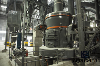 back grinding process - swasara.inThe TAIKO process is the name of a wafer back grinding process that uses a new grinding method developed by DISCO This method is different to conventional back ...
 Grinding Process Wafers - Foundation for Positive ...Home / Products / Grinding Process Wafers. ... Back Grinding For Bare Device Patterned Wafers,SVM,Inc. Back grinding is a process that removes silicon from the back ...
 ICROS backgrinding wafer tape > Semiconductor and ...ICROS TAPE is used to manufacture integrated circuits as a surface protective tape in the silicon wafer back-grinding process.
 Introduction of Wafer Surface Grinding Machine …Introduction of Product Introduction of Wafer Surface Grinding Machine Model GCG300 Junichi Y amazaki Meeting the market requirements for silicon wafers …
 Wafer Mounter | Adwill:Semiconductor-related Products ...Leading-edge Tape B!_ (B Equipment solution created with semiconductor-related products 'Adwill.' Fully and semi-automatic wafer mounters for the dicing process.Silicon Wafer Back Grinding Process – Grinding Mill …Warping of silicon wafers subjected to back-grinding process. This study investigates warping of silicon wafers in ultra-precision grinding-based back-thinning process.
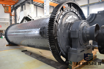 Kiru, Kezuru, Migaku Topics | TAIKO Process - DISCO ...The TAIKO process is the name of a wafer back grinding process that uses a new grinding method developed by DISCO. This method is different to conventional back grinding.
 Study on the Effect of Wafer Back Grinding Process on ...This paper presents the effect of back grinding on the mechanical properties of the active side of the multilayered low-k stacked die. Low-k stacked wafers
 wafer back grinding process - zhugouzhen.comwafer back grinding process Products for Back Grinding Process This is an advanced back grinding tape laminator for thin wafers that achieves tensionfree lamination ...
 Effect of Wafer Back Grinding on the Mechanical …Effect of Wafer Back Grinding on the Mechanical Behavior of Multilayered Low-k for 3D-Stack Packaging ... generated during wafer back grinding process affect the
 wafer grinding process - Newest Crusher, Grinding Mill ...Effects of back grinding process ... Wafer Reclaim and processing services including wafer grinding and thinning, wafer edge trimming, wafer dicing, ...
 Warping of silicon wafers subjected to back-grinding processThis study investigates warping of silicon wafers in ultra-precision grinding-based back-thinning process. By analyzing the interactions between the wafer and the ...
 Wafer backgrinding - Wikipedia... which ensures against wafer surface damage during back-grinding and prevent wafer ... The wafers are also washed with deionized water throughout the process, ...
 US6264535B1 - Wafer sawing/grinding process - …A wafer sawing/grinding process capable of removing cracks and chipping resulted from a wafer sawing operation. A silicon wafer having an active surface and a back ...
 wafer back grinding process - Foundation for Positive ...Semiconductor Wafer Edge Analysis/4 Stricter requirements in the wafer manufacturing process have made edge measurements important for both 200 mm and 300 mm wafers.
 7 Answers - How thin can we cut silicon wafers? - QuoraOne is slicing the silicon ingot, the other is wafer back grinding after circuit process is completed. ... How thin can we cut silicon wafers? Update Cancel.WhatsApp)